Large array multichip modules (MCMs) are playing an increasingly critical role in advanced microelectronic systems, offering higher circuit speeds while significantly reducing size and weight.
These advantages – along with increased circuit densities, cost reductions, and the drive towards miniaturization – are compelling designers to maximize the use of surface space for active devices. These devices often utilize direct die attach techniques, where a die is secured to a substrate in a specific circuit pattern using an adhesive with superior thermal transfer properties. The chips or die are interconnected to the substrate using automatic ball, wedge or ribbon bond techniques, making for a more robust microelectronics assembly.
The adhesive not only anchors the die but also effectively dissipates heat generated by the die, reducing junction temperature and enhancing overall reliability. However, the growing demand for quick turnaround times and high-quality output has heightened concerns about process repeatability.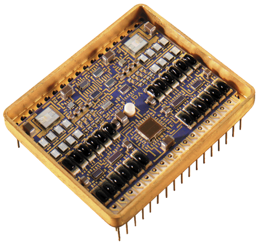
Modern microelectronics assembly houses are equipped with advanced assembly techniques, cutting-edge manufacturing systems, and a wide array of capabilities and services. Today’s customers are more discerning, requiring subcontractors to demonstrate that their processes can consistently meet stringent requirements such as bond line thickness (BLT), void percentage, wire bond/wire pull strength, and ball shear data.
For large, highly integrated dice dissipating up to 30 W, the potential benefits of process characterization hinge on precise control of the adhesive material interface, particularly the BLT. Accurate characterization and process control of the die interface bond line are essential for ensuring a reliable and repeatable assembly process. Variability in the die attach process—especially when adhesive is manually dispensed and die are manually placed—can result in uneven and inconsistent bond lines. However, on highly automated microelectronics production lines, it is possible to achieve consistent thickness, tilt, and void percentage with a high degree of repeatability, provided the process is meticulously characterized. This is particularly crucial in operations where daily output can exceed 500 MCM modules per shift.
Why is BLT so important?
A consistent bond line, free of voids, creates a more reliable die-to-substrate interface, allowing efficient heat dissipation from the die. Typically, the target bond line thickness ranges between 0.001″ and 0.0025″.
When utilizing automated equipment, the following steps can aid in the characterization process:
1. Design an Experiment: Consider the variables involved in the process. Assume the epoxy dispensing portion has been optimized for consistent pattern and volume. Focus on the die attach process, identifying key parameters that may impact the output requirements, such as BLT.
Key parameters for automatic adhesive dispensing include dispense head speed, needle size, and adhesive type. For automatic die attach, key parameters include die size, placement force, dwell time, and adhesive viscosity.
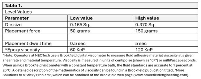
2. Establish Parameter Relationships: Once key parameters are identified, design an experiment to examine how these parameters influence the output requirement—typically, a nominal BLT of 0.0015″. Choose appropriate high and low values for each parameter. For instance, die sizes might range from 0.165″ x 0.165″ to 0.370″ x 0.370″. Table 1 lists these values.
With the parameters set, the experiment can be designed manually or using a statistical process control (SPC) tool like JMP statistical discovery software. SPC tools offer the advantage of easy data analysis. Conducting the experiment is the most effective way to ensure repeatability, quality, and process improvements.
Table 2 outlines the experiment design and the minimum number of runs needed to rigorously evaluate the parameters and their effects on the output. Additional runs using average parameter settings can yield more precise data. It’s advisable to start with fewer runs and expand if necessary.
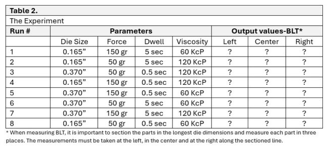
3. Run the Experiments: Set up the automatic die-attach equipment and conduct the eight experiments outlined in Table 2. Use the same die, epoxy, substrate, and equipment as in production. After building the samples, section the parts and measure the bond lines. Input the data into the output values boxes for analysis. Table 3 presents the output values for easier interpretation.
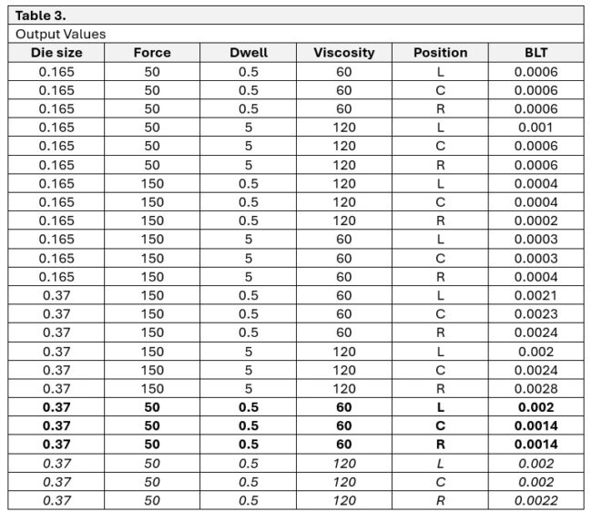
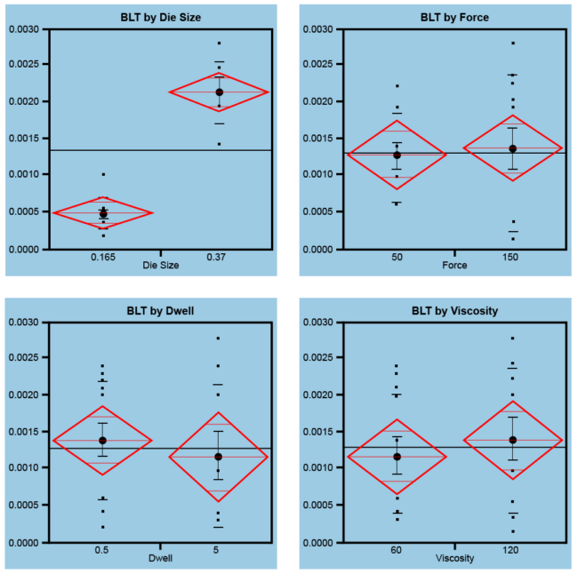
As shown in Table 3, while some parameters met compliance, only the bolded results achieved the desired output targets. Notably, none of the 0.165″ die samples produced compliant results. Analyzing this data using an analysis tool (see Figure 1) revealed that die size had the greatest impact on BLT, but since die size cannot vary, other parameters like dwell time and viscosity were adjusted. Force had the least effect.
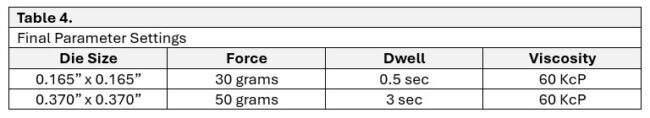
Based on these insights, a second set of experiments was conducted with modified dwell times and force, while maintaining the original die sizes and viscosity at 60 KcP. Viscosity measurements showed no change until the 9th or 10th hour, after which it increased significantly. The final parameter settings, listed in Table 4, successfully achieved the target BLT.
To validate these results, three sets of ten samples were produced using the same settings on different days. Each set was measured to ensure compliance with the target output requirements.
With more than forty years of expertise in high-reliability hybrid and RF technologies, NEOTech has established itself as the largest provider of microelectronics assembly services in North America. We offer a comprehensive array of services encompassing the design, development, and manufacturing of microelectronic assemblies, specializing in microwave electronics and circuits. Our dedicated teams are committed to delivering technical support and advanced testing ensuring superior quality and reliability for our customers.
Visit our Microelectronics Services page for more information about our capabilities.
To get in contact with our Sales team please complete the form at the bottom of this page or link here.
Please feel free to access NEOTech’s design guides for detailed specifications to optimize your design.
Jim Angeloni, NEOTech Microelectronics Process Engineering Fellow
and
Steve Bates, NEOTech Marketing Manager
August 2024
